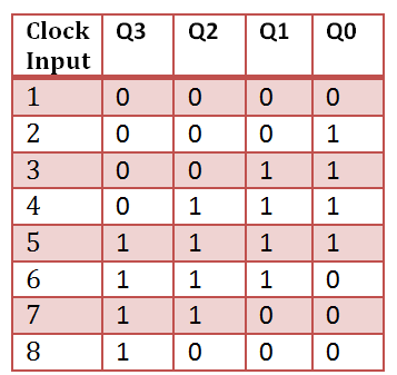
Test Bench Truth Table
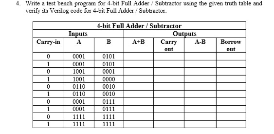
Solved 4 Write A Test Bench Program For 4 Bit Full Adder Chegg Com
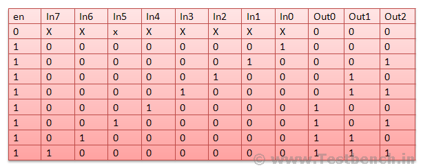
Www Testbench In

Learn Digilentinc Introduction To Vhdl
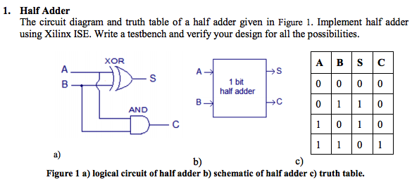
Solved 1 Half Adder The Circuit Diagram And Truth Table Chegg Com
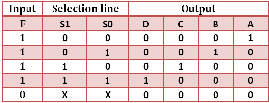
Vhdl Code For 1 To 4 Demux
Verilog Code For Half Adder With Testbench

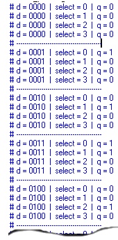
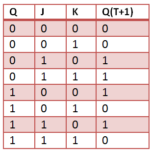
J and k are outputs a b c j k 0 0 0 0 1.
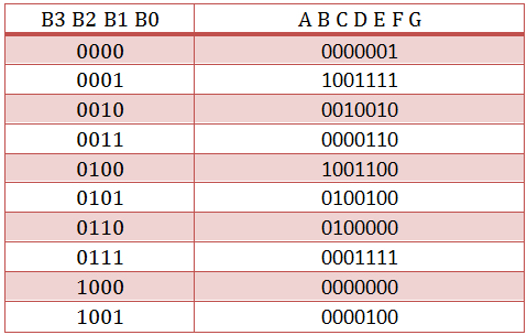
Test bench truth table.

Cs320 Computer Organization And Architecture
Vhdl Code For 2 To 4 Decoder

Verilog For Beginners 3 To 8 Decoder
Multiplexers Different Ways To Implement Verilog By Examples Electrosofts Com
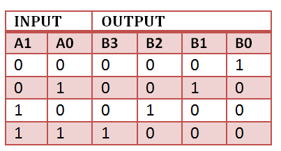
Vhdl Code For 4 To 2 Encoder

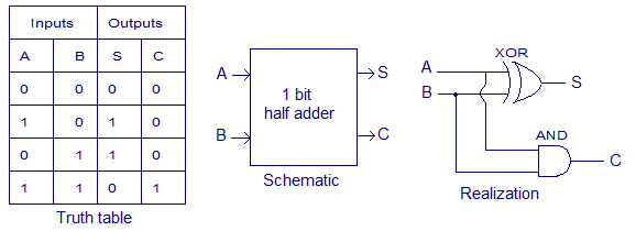
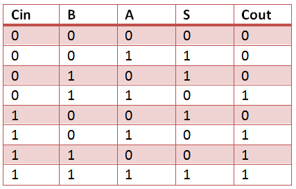
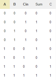
Verilog For Beginners Full Adder

Verilog For Beginners D Flip Flop

Learn Digilentinc Simple Combinational Circuit Design
Verilog Lab Manual Ecad And Vlsi Lab
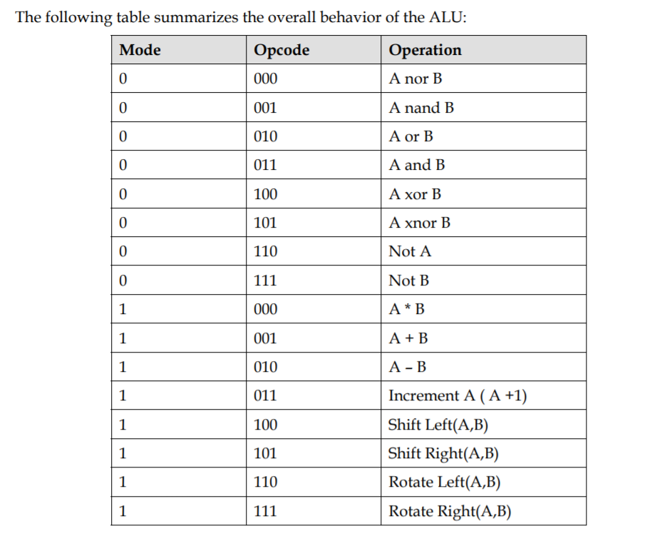
Verilog For Beginners 8 Bit Arithmetic And Logic Unit
Solved Need Vhdl Code And A Testbench Design The 16 Bit Chegg Com

Verilog For Beginners 8 To 1 Multiplexer
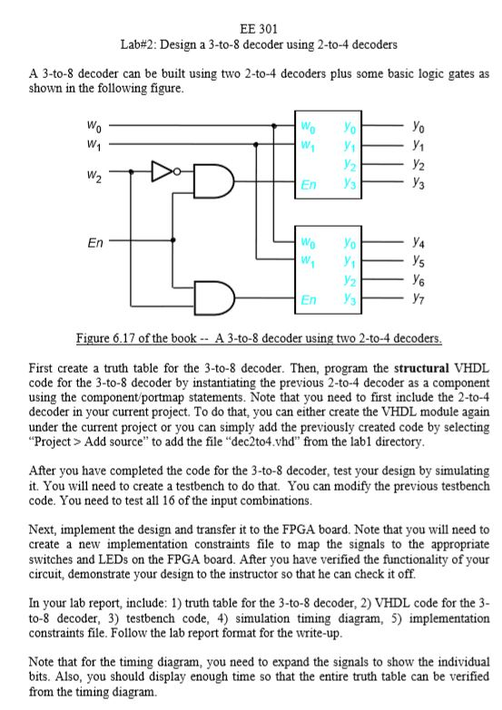
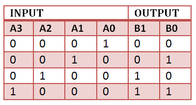
Solved Ee 301 Lab 2 Design A 3 To 8 Decoder Using 2 To 4 Chegg Com
Bcd To 7 Segment Decoder Vhdl Code
Vhdl Code For 4 Bit Ring Counter And Johnson Counter

Verilog Code For 2 1 Multiplexer Mux All Modeling Styles
Vhdl Code For Flipflop D Jk Sr T
Http Users Wpi Edu Rjduck Vivado 20simple 20vhdl 20test 20bench Pdf
Https Encrypted Tbn0 Gstatic Com Images Q Tbn 3aand9gct7af7svohvnsry J6mit7aeidn8pyshkvuweadvmdjar8 6lbv Usqp Cau
Vhdl Code For Full Adder
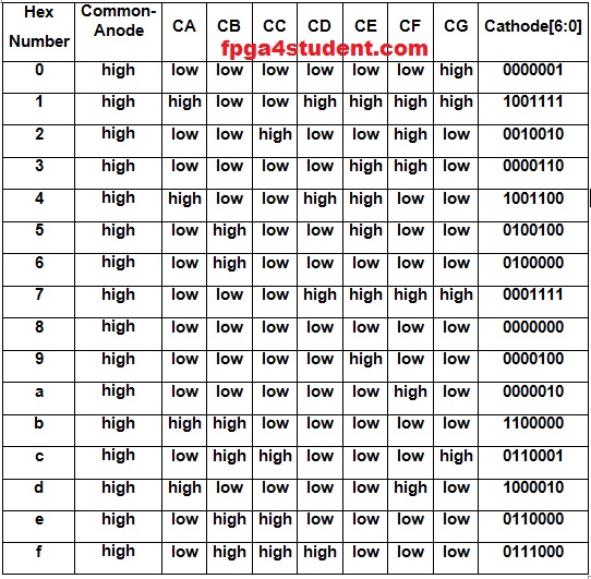
Vhdl Code For Seven Segment Display On Basys 3 Fpga Fpga4student Com
3 Input Exclusive Nor Gate Truth Table Logic Arduino Gate
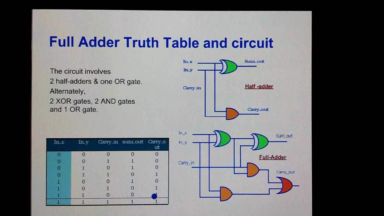
Full Adder Circuit Truth Table And Verilog Code Youtube
Parallel Adder 4 Bit Electronics Hub
Source : pinterest.com
